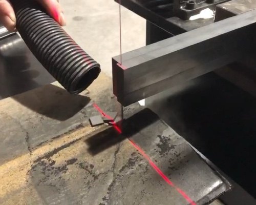
At present, as early as 2016, the global monocrystalline silicon wafer producers have basically switched from traditional mortar cutting (silicon carbide powder, steel wire, polyvinyl alcohol mixture) to diamond wire cutting, which has greatly reduced the cost of monocrystalline silicon wafers, resulting in a certain cost-effectiveness advantage in the competition with multicrystalline silicon wafers. Therefore, multicrystalline silicon wafers must be switched to diamond wire slicing as soon as possible. Polycrystalline silicon wafer companies that do not switch will face the dilemma of being unable to survive. So the question is, how much do you know about diamond wire cutting? Let’s learn more about it together~
Diamond cutting wire technology is currently divided into two main types, namely resin diamond wire and electroplated diamond wire.
The main difference between electroplated diamond wire and resin diamond wire is the fixing method of diamond particles and the difference in coating. Resin diamond wire uses resin as the wrapping material, and electroplated diamond wire uses metal coating (generally nickel and nickel-cobalt alloy) as a binder. Both have their own advantages and disadvantages in terms of production cost and durability.
As a new cutting technology, diamond cutting wire technology has the advantages of improving the cutting rate, reducing silicon wafer loss, and reducing sewage discharge. It can greatly reduce the cost of silicon wafer manufacturers. At present, diamond cutting wire technology is gradually replacing the old mortar cutting technology in the silicon wafer production industry. Development status of diamond wire cutting equipment
At present, domestic silicon wafer multi-wire cutting equipment is still dominated by foreign brands. After more than ten years of continuous innovation and improvement, the new generation of foreign multi-wire cutting machines have shown more superior characteristics:
1. The cutting wire used is thinner and the silicon wafer is thinner, which greatly reduces the consumption of silicon raw materials. The thickness of silicon wafers has been reduced from the original 330μm to 180-220μm. And there is still room for further development. It is possible to reduce the thickness of silicon wafers from 180μm to 150μm in a short period of time, and further reduce the manufacturing cost by 25%.
2. Increase the line speed to more than 1000m/min; increase the feed speed to 1-5mm/min; and increase the production efficiency by 2-3 times.
3. Equipped with a more precise CNC system, with advanced and reasonable process control and cutting line tension control and monitoring system.


